SanRex 50 Seaview Blvd. Port Washington, NY 11050-4618 PH.(516)625-1313 FAX(516)625-8845 E-mail: semi@sanrex.com
PK
(PD,PE)
250HB
THYRISTOR MODULE
UL;E76102
M
92
12
18
M8◊14
110TAB
2.8.0.5T
80±0.3
42max
34max
2
26
60
48
24
5
5
K1G1
K2G2
12
26
7
4-6M5
R8.0
33
52
Unit
A
Symbol
Item
Conditions
Ratings
250
Unit
I
T
AV
Average On-State Current
I
T
RMS
R.M.S. On-State Current
Single phase, half wave, 180
∞conduction, Tc72
Single phase, half wave, 180
∞conduction, Tc72
I
TSM
Surge On-State Current
I
2
t
I
2
t
P
GM
Peak Gate Power Dissipation
P
G
AV
Average Gate Power Dissipation
I
FGM
Peak Gate Current
V
FGM
Peak Gate Voltage
Forward
1
2
cycle, 50Hz/60Hz, peak Value, non-reqetitive
Value for one cycle of surge current
A
390
A
5000/5500
A
125000
10
A
2
S
W
3
V
RGM
Peak Gate Voltage
Reverse
di/dt
Critical Rate of Rise of On-State Current
I
G
100mATj25V
D
1
2
V
DRM
dI
G
/dt0.1A/s
V
ISO
Isolation Breakdown Voltage R.M.S.
Tj
Operating Junction Temperature
Tstg
Storage Temperature
Mounting
Torque
Mass
Mounting
M5
Terminal
M8
A.C. 1 minute
Recommended Value 1.5-2.5
15-25
Recommended Value 8.8-10
90-105
Typical Value
3
W
A
10
V
5
V
200
A/
s
2500
V
-40 to 125
-40 to 125
2.7
28
11
115
510
N
fB
g
Symbol
Item
Conditions
Ratings
50
Unit
I
DRM
Repetitive Peak Off-State Current, max.
I
RRM
Repetitive Peak Reverse Current, max.
at V
DRM
, Single phase, half wave, Tj
125
at V
DRM
, Single phase, half wave, Tj
125
V
TM
Peak On-State Voltage, max.
I
GT
/V
GT
Gate Trigger Current/Voltage, max.
V
GD
Non-Trigger Gate, Voltage. min.
tgt
Turn On Time, max.
dv/dt
Critical Rate of Rise of Off-State Voltage, min.
I
H
Holding Current, typ.
On-State Current 750A, Tj
125 Inst. measurement
Tj
25I
T
1AV
D
6V
mA
50
mA
1.60
V
100/3
Tj
125V
D
1
2
V
DRM
I
T
250AI
G
100mATj25V
D
1
2
V
DRM
dI
G
/dt0.1A/s
0.25
mA/V
V
10
Tj
125V
D
2
3
V
DRM
Exponential wave.
Tj
25
I
L
Lutching Current, typ.
Rth
j-cThermal Impedance, max.
Tj
25
Junction to case
500
s
V/
s
50
mA
100
mA
0.14
/W
Electrical Characteristics
Maximum Ratings
Symbol
Item
PK250HB120
PD250HB120
PE250HB120
Ratings
PK250HB160
PD250HB160
PE250HB160
Unit
V
RRM
Repetitive Peak Reverse Voltage
1200
1600
V
1300
1700
V
1200
1600
V
V
RSM
V
DRM
Non-Repetitive Peak Reverse Voltage
Repetitive Peak Off-State Voltage
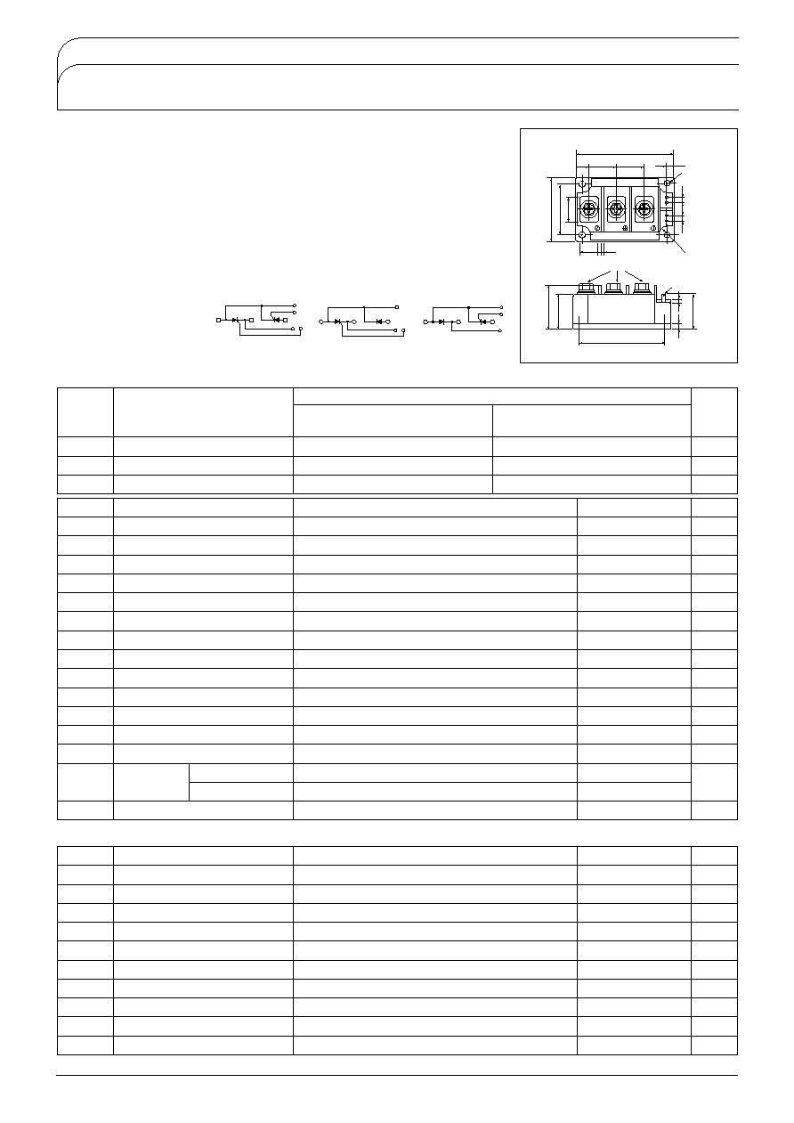
markThyristor and Diode part. No markThyristor part
Power Thyristor/Diode Module PK250HB series are designed for various rectifier
circuits and power controls. For your circuit application. following internal connections
and wide voltage ratings up to 1,600V are available.
Isolated mounting base
I
T
AV
250A, I
T
RMS
310A, I
TSM
5500A
di/dt 200 A/
s
dv/dt 500V/
s
Applications
Various rectifiers
AC/DC motor drives
Heater controls
Light dimmers
Static switches
Internal Configurations
K1
A2
K2
A1K2
G1
K2
G2
1
2
3
K1
A2
K2
A1K2
G1
K2
1
2
3
K1
A2
K2
A1K2
K2
G2
1
2
3
PK
PD
PE
PK(PD,PE)250HB
;;
-
Peak Forward Gate Voltag10V
Pe
ak G
ate
P
ow
er
1
0W
Ave
ra
ge G
ate
P
ow
er3
W
Peak Gate Current
3
A
Maximum Gate Non-Trigger Voltage
125
25
-30
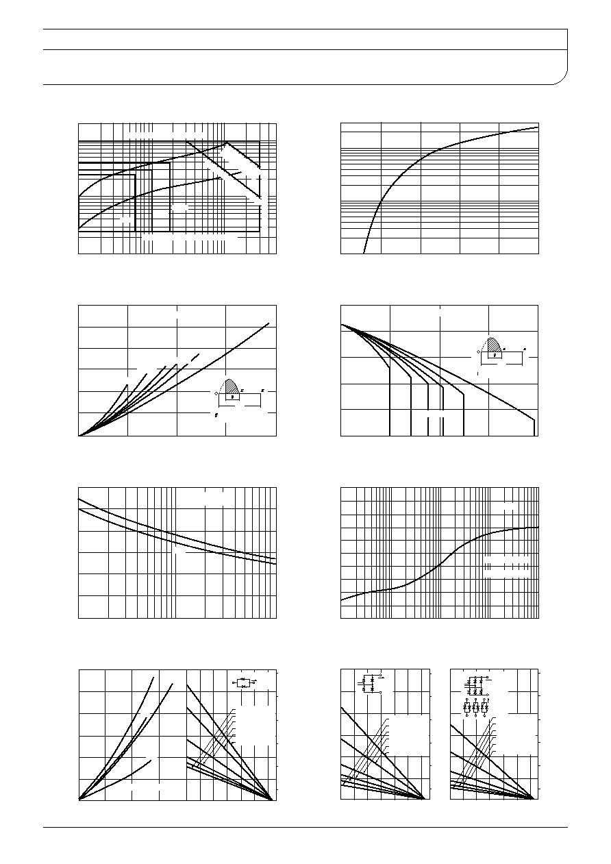
Gate Characteristics
Gate CurrentmA
Gate Voltage
V
Tj125
On-State Characteristics
On-State VoltageV
On-State Current
A
D.C.
: Conduction Angle
360
2
Per one element
180
120
90
60
30
Average On-State Current Vs Power Dissipation
Single phase half wave
Average On-State CurrentA
Power Dissipation
W
: Conduction Angle
360
2
Per one element
180
120
90
60
30
D.C.
Average On-State Current Vs Maximum Allowable
Case TemperatureSingle phase half wave
Average On-State CurrentA
Conduction Angle
Allowable Case Temperature
Per one element
60Hz
50Hz
Surge On-State Current Rating
Non-Repetitive
Timecycles
Surge On-State Current
A
start
-
-
-
Maximum
Junction to Case
Per one element
Transient Thermal Impedance
Time
t
sec
Transient Thermal Impedance
j-c
/
W
Rth f-a:0.5/W
Rth f-a:0.4/W
Rth f-a:0.3/W
Rth f-a:0.2/W
Rth f-a:0.1/W
Rth f-a:0.05/W
Conduction Angle 180∞
W3
B6
B2
W1
Output Current
Output CurrentA
Ambient Temperature
WBidirectional connection
Total Power Dissipation
W
Allowable Case Temperature
IdAr.m.s.
Rth f-a:0.5/W
Rth f-a:0.4/W
Rth f-a:0.3/W
Rth f-a:0.2/W
Rth f-a:0.1/W
Rth f-a:0.05/W
Rth f-a:0.5/W
Rth f-a:0.4/W
Rth f-a:0.3/W
Rth f-a:0.2/W
Rth f-a:0.1/W
Rth f-a:0.05/W
BTwo Pluse bridge connection
Ambient Temperature
Ambient Temperature
BSix pulse bridge connection
Three phase
bidiretional connection
Allowable Case Temperature
IdAav.
IdAr.m.s.
IdAav.